Show this simple video it is very useful to understand basic functionality of transistor.
About VLSI concepts
Tuesday 25 August 2015
Sunday 31 May 2015
Universal Property of NAND and NOR Gates
Universal property :
NAND and NOR gates possess a special property: they are universal. That is, given enough gates, either type of gate is able to mimic the operation of any other gate type. For example, it is possible to build a circuit exhibiting the OR function using three interconnected NAND gates as shown in below. The ability for a single gate type to be able to mimic any other gate type is one enjoyed only by the NAND and the NOR. In fact, digital control systems have been designed around nothing but either NAND or NOR gates, all the necessary logic functions being derived from collections of interconnected NANDs or NORs.
 step1 step2
As shown in above figure
step 1 :
A . A = A (Idempotent law)
complement (A.A ) = complement (A)
step2 :
complement ( complement(A) ) = A (double negation law)
complement (A . B) = complement (A) + complement (B) (deMorgan's law)
complement ( complement(A) . complement(B) ) = complement ( complement(A) ) + complement (complement (B))
= A + B (OR of A,B)
Universal property of NAND Gates :
Universal property of NOR Gates :
NAND and NOR gates possess a special property: they are universal. That is, given enough gates, either type of gate is able to mimic the operation of any other gate type. For example, it is possible to build a circuit exhibiting the OR function using three interconnected NAND gates as shown in below. The ability for a single gate type to be able to mimic any other gate type is one enjoyed only by the NAND and the NOR. In fact, digital control systems have been designed around nothing but either NAND or NOR gates, all the necessary logic functions being derived from collections of interconnected NANDs or NORs.

As shown in above figure
step 1 :
A . A = A (Idempotent law)
complement (A.A ) = complement (A)
step2 :
complement ( complement(A) ) = A (double negation law)
complement (A . B) = complement (A) + complement (B) (deMorgan's law)
complement ( complement(A) . complement(B) ) = complement ( complement(A) ) + complement (complement (B))
= A + B (OR of A,B)
Universal property of NAND Gates :
Universal property of NOR Gates :
Friday 29 May 2015
Laws followed in digital electronics
Laws followed by digital electronics :
Annulment Law :
if A (is unknown value, means whether 0 or 1) is AND'ed with 0 then result always equal to 0.
if A is OR'ed with 1 then the result always equal to 1.
A . 0 = 0
A + 1 = 1
Identity Law :
The result always equal to A when A is OR'ed with 0 or if A is AND'ed with 1.
A . 1 = A
A + 0 = A
Idempotent Law :
The result is always equal to A when OR'ed or AND'ed with A itself.
A + A = A
A . A = A
Complement Law :
The result is always equal to 0 when AND'ed with complement of itself.
The result is always equal to 1 when OR'ed with complement of itself.
A . ABAR = 0
A + ABAR = 1
Commutative Law :
The order of application of two separate inputs is not important.
A + B = B+ A
Double Negation Law :
if A is two times complemented it gives same value.
complement (complement ( A) ) = A
de Morgan's Law:
Law1 : NOR'ed of two inputs is equal to AND'ed of complement inputs.
Law2 : NAND'ed of two inputs is equal to OR'ed of complement inputs.
complement (A + B) = complement(A) . complement(B)
complement (A . B ) = complement(A) + complement(B)
Tuesday 7 April 2015
Logic Gates
NAND Gate :
it is logic gate, any input is low then output is high.
 single word : compliment of and gate
NOR Gate :
it is logic gate, any input is high then output is low.
 single word : compliment of or gate.
XOR Gate :
it is a logic gate, which performs exclusive or operation.

single word : output is high only when two inputs different.
XNOR Gate :
it is a logic gate, which performs exclusive nor operation.

it is logic gate, any input is low then output is high.
NOR Gate :
it is logic gate, any input is high then output is low.
XOR Gate :
it is a logic gate, which performs exclusive or operation.
single word : output is high only when two inputs different.
XNOR Gate :
it is a logic gate, which performs exclusive nor operation.
single word : output is high only when two inputs same.
Monday 6 April 2015
Logic Gates
Logic Gates :
A logic gate is an idealized or physical device implementing a Boolean function; that is, it performs a logical operation on one or more logical inputs, and produces a single logical output.
Logic gates are primarily implemented using diodes or transistors acting as electronic switches
AND Gate :
The AND gate is a basic digital logic gate that implements logical conjunction.
 |
| AND GATE |
Single word : Output high only when all inputs high.
OR Gate :
The OR gate is a digital logic gate that implements logical disjunction.
| OR GATE |
NOT Gate :
NOT gate is a logic gate which implements logical negation.

Single Word : Output is inversion of input.
Friday 3 April 2015
Basic Elements
Diode :
A diode is a basic electrical device which is used as rectifier which converts an alternating current into a direct one by allowing a current to flow through it in one direction only.
 |
| Diode |
Transistor :
. A bipolar transistor has terminals labeled base, collector, and emitter. A small current at the base terminal (that is, flowing between the base and the emitter) can control or switch a much larger current between the collector and emitter terminals. For a field-effect transistor, the terminals are labeled gate, source, and drain, and a voltage at the gate can control a current between source and drain.
BJT :
FET :
BJT :
FET :
Friday 27 March 2015
About Doping in semiconductors
Doping :
Doping is the process of adding impurities to intrinsic semiconductor materials to change electrical properties like carrier concentration. Doped semiconductor material is also called as extrinsic semiconductor. Depends on conductivity requirements doping levels may be changed. A semiconductor doped in high levels that it acts more like a conductor than a semiconductor is referred to as degenerate.
Effects after doping :
The most important factor that doping directly affects is the material's carrier concentration. In an intrinsic semiconductor under thermal equilibrium, the concentration of electrons and holes is equivalent. That is,
n = p = n_i
If we have a non-intrinsic semiconductor in thermal equilibrium the relation becomes (for low doping):
n_0 * p_0 = n_i^2
where n_0 is the concentration of conducting electrons, p_0 is the electron hole concentration, and n_i is the material's intrinsic carrier concentration. Intrinsic carrier concentration varies between materials and is dependent on temperature.
An increase in doping concentration affords an increase in conductivity due to the higher concentration of carriers available for conduction. Degenerate (very highly doped) semiconductors have conductivity levels comparable to metals and are often used in modern integrated circuits as a replacement for metal. Often superscript plus and minus symbols are used to denote relative doping concentration in semiconductors. For example, n+ denotes an n-type semiconductor with a high, often degenerate, doping concentration. Similarly, p− would indicate a very lightly doped p-type material.
The Group IV semiconductors such as diamond, silicon, germanium, silicon carbide, and silicon germanium, the most common dopants are acceptors from Group III or donors from Group V elements. Boron, arsenic, phosphorus, and occasionally gallium are used to dope silicon.
By doping pure silicon with Group V elements such as phosphorus, extra valence electrons are added that become unbonded from individual atoms and allow the compound to be an electrically conductive n-type semiconductor.
By doping with Group III elements, which are missing the fourth valence electron, creates "broken bonds" (holes) in the silicon lattice that are free to move. The result is an electrically conductive p-type semiconductor.
In this context, a Group V element is said to behave as an electron donor, and a group III element as an acceptor.
 |
| After Doping |
In Single word : Adding impurities
Tuesday 24 March 2015
About Semiconductors & Types
A semiconductor material has an electrical conductivity value falling between that of a conductor, such as copper, and an insulator, such as glass. Semiconductors are the foundation of modern electronics. Semiconducting materials exist in two types - elemental materials and compound materials.
Generally we have different types of semiconductors based on properties in that
1. intrinsic semiconductor
2. Extrinsic semiconductor
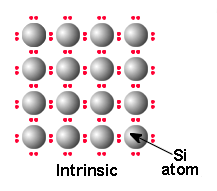
Intrinsic semiconductors :
An intrinsic semiconductor material is also called as undoped semiconductor or i-type semiconductor, is chemically very pure and possesses poor conductivity. It has equal numbers of negative carriers (electrons) and positive carriers (holes). A silicon crystal is different from an insulator because at any temperature above absolute zero temperature, there is a finite probability that an electron in the lattice will be knocked loose from its position, leaving behind an electron deficiency called a "hole".
by we applying external energy (voltage,temperature) both the electrons and the holes can contribute small current flow.

Generally we have different types of semiconductors based on properties in that
1. intrinsic semiconductor
2. Extrinsic semiconductor
Intrinsic semiconductors :
An intrinsic semiconductor material is also called as undoped semiconductor or i-type semiconductor, is chemically very pure and possesses poor conductivity. It has equal numbers of negative carriers (electrons) and positive carriers (holes). A silicon crystal is different from an insulator because at any temperature above absolute zero temperature, there is a finite probability that an electron in the lattice will be knocked loose from its position, leaving behind an electron deficiency called a "hole".
by we applying external energy (voltage,temperature) both the electrons and the holes can contribute small current flow.
In Single Word : pure semiconductor
Extrinsic Semiconductor :
Where as an extrinsic semiconductor is an improved intrinsic semiconductor with a small amount of impurities added by a process, known as doping, which alters the electrical properties of the semiconductor and improves its conductivity. Introducing impurities into the semiconductor materials (doping process) can control their conductivity.
Sunday 22 March 2015
About solid state materials
Solid-state materials can be classified into three groups:
1. insulators
2. semi conductors
3. conductors
Insulators :
Insulators are those materials that don't conduct electricity under normal conditions. For instance: air is an insulator. You don't get electrocuted when approaching a plug point since air is an insulator.
. The outer most orbit of an atom can be divided into various sub orbitals or bands. As you can see I have divided into three colors. The lower most band is called a valence band. The electrons in this band determine the valency of the atom. The upper most band is called the conduction band. In this band, the electron is farthest from the positively charged nucleus and is capable of easily escaping out of the atom and thus enabling the material / atom to conduct electricity.
Single Word : zero conductivity

semiconductors :
Semiconductors are materials that behave like both conductors and insulators. In certain condition a semiconductor acts like a conductor. For example charcoal and graphite which are allotrope of Carbon act as conductor. Whereas diamond which has a different crystal structure act as an insulator. The conductivity of semiconductors can be increased by adding certain impurities to them this is called doping. The conductivity may increase by pumping energy into semiconductor crystal in the form of heat or light.

Conductors :
Conductors are substances that easily let electrical charge pass through them with relatively very-less resistance. Almost all metals are conductors. When ever you cut an electric wire, you can see copper or some other metal at its core. Its because these metals can easily conduct electricity.
there is no forbidden energy gap. The valence and conduction band are overlapping each other. Hence its extremely easy for electrons to move from valence to conduction band. Hence conductors easily conduct electricity without much loss of energy. They conduct electricity under normal conditions.

Single word : External influence is not required to conducts.
Subscribe to:
Posts (Atom)