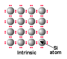
Doping :
Doping is the process of adding impurities to intrinsic semiconductor materials to change electrical properties like carrier concentration. Doped semiconductor material is also called as extrinsic semiconductor. Depends on conductivity requirements doping levels may be changed. A semiconductor doped in high levels that it acts more like a conductor than a semiconductor is referred to as degenerate.
Effects after doping :
The most important factor that doping directly affects is the material's carrier concentration. In an intrinsic semiconductor under thermal equilibrium, the concentration of electrons and holes is equivalent. That is,
n = p = n_i
If we have a non-intrinsic semiconductor in thermal equilibrium the relation becomes (for low doping):
n_0 * p_0 = n_i^2
where n_0 is the concentration of conducting electrons, p_0 is the electron hole concentration, and n_i is the material's intrinsic carrier concentration. Intrinsic carrier concentration varies between materials and is dependent on temperature.
An increase in doping concentration affords an increase in conductivity due to the higher concentration of carriers available for conduction. Degenerate (very highly doped) semiconductors have conductivity levels comparable to metals and are often used in modern integrated circuits as a replacement for metal. Often superscript plus and minus symbols are used to denote relative doping concentration in semiconductors. For example, n+ denotes an n-type semiconductor with a high, often degenerate, doping concentration. Similarly, p− would indicate a very lightly doped p-type material.
The Group IV semiconductors such as diamond, silicon, germanium, silicon carbide, and silicon germanium, the most common dopants are acceptors from Group III or donors from Group V elements. Boron, arsenic, phosphorus, and occasionally gallium are used to dope silicon.
By doping pure silicon with Group V elements such as phosphorus, extra valence electrons are added that become unbonded from individual atoms and allow the compound to be an electrically conductive n-type semiconductor.
By doping with Group III elements, which are missing the fourth valence electron, creates "broken bonds" (holes) in the silicon lattice that are free to move. The result is an electrically conductive p-type semiconductor.
In this context, a Group V element is said to behave as an electron donor, and a group III element as an acceptor.
 |
| After Doping |
In Single word : Adding impurities